Welcome to the web page of the Organic Electronics Laboratory, the research group at the Slovak University of Technology.
We are interested in the study of material properties, device fabrication technology, and characterisation techniques related to organic and flexible electronics. Our research topics include applications in energy harvesting, internet-of-things, or healthcare. The lab is equipped by vacuum deposition as well as printing technologies localised in the Clean rooms of Institute of Electronics and Photonics, Slovak University of Technology.
Members
Prof. Martin Weis, DrSc.(martin.weis@stuba.sk)
Martin is a senior researcher and head of Organic Electronics Lab at the Institute of Electronics and Photonics of STUBA. He is a professor from 2020, while higher doctorate (Doctor of Science) received in 2018. In the past, he was a member of Slovak Academy of Sciences and visiting scholar of Tokyo Institute of Technology. His research is focused on organic electronics, nanotechnology, and advanced materials.
Awards:
– Prize for scientific impact awarded by Slovak Physical Society (2019)
– Top reviewer awards: Top reviewers in Cross-Field (2019), Top reviewers for Physics and Astronomy (2017), Top reviewers for Mathematics (2017), Sentinels of Science: Materials Science (2016)
– Best publication of the Slovak University of Technology (2014)
– Award of the Minister of Education, Science, Research and Sport of Slovak Republic – Scientist of the year 2013 up to 35 years of age (2013)
– Stefan Schwarz supporting fund fellowship holder at Slovak Academy of Sciences (2009-2013)
– Award Scientist of the year 2012 at Slovak University of Technology
– Postdoctoral Fellowships for Foreign Researchers of Japanese Society for Promotion of Science (2007-2009).
– the International Union for Vacuum Science, Technique and Applications (IUVSTA), a representative member of Slovakia in Surface Engineering Division
– program committees of “International Conference on Organic Electronics” (2016-2020); “IEEE International Reliability Physics Symposium” (2017, 2018); “European Conference on Organized Films” (2013-2019); “European Symposium on Reliability of Electron Devices, Failure Physics and Analysis” (2019-2020).
– the excellent research team in the field of electrical engineering for “Advanced materials, technologies, and structures for progressive micro/nano electronic and photonic devices and systems”, recognized by the accreditation commission of Slovak Republic.
Dr. Michal Micjan (michal.micjan@stuba.sk)
Michal is a researcher and project manager of Organic Electronics Lab of Institute at Electronics and Photonics of STUBA. Michal is a young researcher in organic electronics, device design and characterization devices. He is responsible for research and development in the design and characterization of electronic transistors. He has extensive experience with several deposition technologies of organic electronics as well as their characterization. As a principal investigator Michal received several national grants (Tatra banka Foundation 2019, Axa Innovator 2018, internal grants of STU). Despite his young age, he has extensive experience in the management of national (APVV) and international projects (at the level of the partner organization). Michal is also an active member of the research team in several national and international projects (VEGA, APVV, DAAD, H2020).
Dr. Miroslav Novota(miroslav.novota@stuba.sk)
Miroslav received his PhD (2019) in Electronics and Photonics from the Slovak University of technology in Bratislava (Slovakia). His PhD Thesis was focused on the development of technologies for organic semiconductor-based integrated circuits. Miroslav is currently a researcher scientist in the laboratory of Professor Martin Weis at the department of Organic Electronics, Faculty of Electrical Engineering and Information Technology, Slovak University of Technology in Bratislava. Always of great interest for Miroslav are both the fundamental and applied research on novel organic materials, development of sensoric structures and integrated circuits based on organic materials, with a particular interest in technology of deposition of thin layers by evaporation and wet tchniques.
Dr. Juraj Nevrela(juraj.nevrela@stuba.sk)
Juraj received his BS and MSc degrees at Slovak University of Technology (STU), Faculty of Electrical Engineering and Information Technology, Focusing his aim of research on the area of conductive polymers and pattering technologies. Main breakthrough of his science career at STU, was enhancing conductivity of PEDOT:PSS and implemented progressive nanoimprint technique to the university technological roadmap. Nowadays Juraj works on the research of printed electronics via inkjet printing.
MSc. Tomas Vincze (tomas.vincze@stuba.sk)
Tomas is a young researcher of Organic Electronics Lab of Institute of Electronics and Photonics of STUBA. Tomas is mainly engaged in research in the field of thin film transistors based on sol gel technology. Tomas has also few years’ experience with measurement of Raman spectroscopy as well as measurement of layer thickness based on profilometry DEKTAK.
MSc. Michal Hanic (michal.hanic@stuba.sk)
Michal is a new researcher of Organic Electronics Lab of Institute of Electronics and Photonics of STUBA. Michal is mainly engaged in research in the field of characterisation of organic field-effect transistors. Michal is also responsible for the design of hardware solutions, as well as prototype a measurement system devices fabrication.
MSc. Vratislav Rezo
Vratislav is a young researcher of Organic Electronics Lab of Institute of Electronics and Photonics of STUBA. Vratislav is mainly engaged in research in the field of flexible electronic based on ink-jet printed technology. Vratislav is also responsible for the design of hardware and software solutions, as well as prototype device fabrication.
MSc. Michal Sobota
Michal is a young researcher of Organic Electronics Lab of Institute of Electronics and Photonics of STUBA. Michal is focusing on passivation of organic electronics devices, preparation of thin layer using by vacuum evaporation or spincoating and measurement of thin-films thickness.
BSc. Adam Vardzak
Adam
is a young researcher of Organic Electronics Lab of Institute of Electronics
and Photonics of STUBA. Adam is mainly engaged in research in the field of flexible
sensors based on ink-jet printed technology.
Ondrej Kokavec
Ondrej is a young researcher of Organic Electronics Lab of Institute of Electronics and Photonics of STUBA. Ondrej is mainly engaged in research in organic light-emitting diodes.
Lab description
Available materials:
Organic materials – standard n– and p-type small-molecule organic semiconductors (e.g. pentacene, fullerene, phthalocyanines, etc) as well as polymer organic semiconductors (e.g. P3HT, MEH-PPV). Conductive polymer PEDOT:PSS is applicable for thin, transparent, flexible and conductive layers (100 Ω/sq for 50 nm thick film).
Nanoparticles (NPs) – dielectric (high-k), semiconducting, or metal (plasmonic) NPs can be applied. We have experience with NP surface modification and depositions. Preparation of plasmonic NP monolayers from colloids as well as by vacuum methods with controlled optical properties also possible.
Substrates – Si wafers, sapphire, glass, or flexible plastic substrates.
Encapsulation – besides standard inorganic encapsulation methods we can provide flexible, transparent barrier coating based on parylene C.
Technologies:
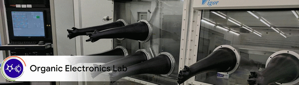
Vacuum evaporation systems – for deposition of organic and inorganic materials in high vacuum through shadow masks. The deposition system (SPECTROS 100) comprising the in situ simultaneous evaporation of 8 organic materials and metals from 3 different sources is available. The system is connected with glove-box assembly suitable for fabrication of sensitive devices as well as measurement in a nitrogen atmosphere.
Wet deposition techniques – besides standard dip-coating or spin-coating the lab is also equipped the rare spin-coating system with the chuck heated up to 250°C, which enables deposition of low-soluble materials or high crystallinity layer. The organic inkjet printer (Dimatix) is also available for deposition by printing.
Patterning – Carl Suss aligner with 0.4μm resolution (deep UV) with both sides aligning and nanoimprint lithography module.
Characterisation methods:
Electrical – All standard methods such as I-V, C-V, impedance spectra, DLTS, or noise analysis
Optical – Electroluminescence, solar simulator for solar cells, microRaman, various modes of SEM.
Analytical – AFM, STM, SEM.
Theory, Modelling and Simulation:
Optical properties – Simulation of light transmission or scattering for thin films, nanostructured surfaces, plasmonics, LEDs (far-fields), photonic structures and waveguides.
Electrical properties – Analysis of charge transport, contact resistance, and defects (deep levels) in organic devices.